- -52%

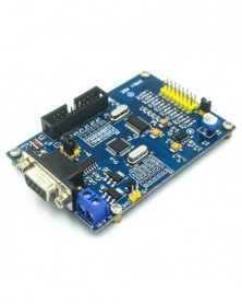
ADS1256 24 bites AD nagy pontosságú adatgyűjtő modul 24 bites ADC STM32F103C8T6 AD modul
ADS1256 24 bites AD nagy pontosságú adatgyűjtő modul 24 bites ADC STM32F103C8T6 AD modul
1 739 Ft
52% megtakarítás
3 623 Ft
Nincs adó
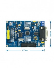
1. power input terminal, input voltage range 5.5V - 12V (5V power supply, please connect directly to 2);
10. power indicator light LED;
2. 5V power supply input terminal (1.2 two power supply, only one can);
11. JTAG interface, designed by the definition of JLINK-V8 or V9;
3. STM32F103C8T6 leads to GPIO, which is convenient for the development of two times. The silk screen is directly corresponding to the pin number of the chip.
12. unmarked;
4. new original master control MCU: STM32F103C8T6;
13. STM32F103C8T6 reset button;
5. 2.5V datum, ultra high precision, low temperature floating;
14. USB to TTL connection, corresponding to MCU TX, RX, GND, can communicate directly with the computer;
6. adjustable potentiometer, output adjustable voltage link to AIN0/ I0;
15. imported 3232 serial port communication chip;
7. the 8 channels of input are collected, the I0-I7 is connected to the positive end of the acquisition voltage, and the G is simulated, and the negative end of the acquisition voltage is connected.
16. serial port, mother head;
8. input filter and attenuation resistance, default does not do attenuation, leave the position of welding attenuation resistance, 0603 package;
17. the output voltage of the adjustable potentiometer is controlled by I0 / AIN0: disconnecting the IO suspension, and measuring the output voltage end of the adjustable potentiometer by I0;
9. ADS1256IDB collection chip, new original import;
18. STM32 BOOT0 and BOOT1 select control jump cap;
The results show that the unit of attention is uV
As shown in the following chart, the acquisition card is charged on the card, and the seventh uses the channel I7 and the simulated AGND (G) to use the jump cap short to measure the simulated ground. The size of the measurement results directly reacts to the layout and wiring of the plate, and the filter is good or bad. The smaller the better the result, the smaller the better the fluctuation. For multiple sample tests, the sampling voltage is at several uV. Many other boards on the market have several hundred uV of the ground sampling voltage, and this sampling voltage will be directly coupled to the subsequent sampling results, resulting in a loss of precision.
12

Szállításii feltételek

Biztonsági feltételek

Visszaküldési feltételek


