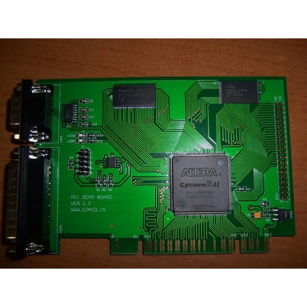
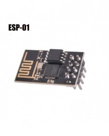
S1300 PCI FPGA development experiment board adopts PCI interface to facilitate user to develop independently.
Users can design and apply plug - in, such as external A/D data acquisition,
The application of the system of image data processing, and so on, does not need to have too much understanding of the PCI interface.
The development board is compatible with the FPGA development board of the iridium element company's fire dragon knife series, and the price is very cheap.
The core FPGA chip uses the new CYCLONE FPGA series of ALTERA company.
EP1C6Q240C8 (standard configuration) /EP1C12Q240C8 with 6000/12000 logical macro units, respectively.
It is equivalent to a standard 150 thousand /30 million logic gate circuit with a speed of -8, and the speed of the compiled system can reach 100MHz,
It can support the development of ALTERA's SOPC kernel NIOS2 system, and the NIOS2 development environment compiled
Executable files can be downloaded through the PCI interface to the FLASH on the development board,
Provide free ALTERA QUARTUS2 4.1 and NIOS2 1.01 development tool discs free of charge,
The development board supports AS and PS downloads, and provides free ALTERA with the development board
BYTEBLASTER 2 downloads a cable for users to use.
Provide NIOS2 CPU development guide and technical support,
The external bus interface of the PCI interface motherboard supports 8, 16, and 32 bit data buses, which can be directly with CPU,
SDRAM, FIFO, external interface chip and other devices are directly connected.
The following is the internal IP core interface of the FPGA development board:
PCI bus 2.2 standard, 32 bit bus, complete VHDL source code design,
Support PCI bus configuration reading, configuration writing,
Support PCI bus IO reading, IO writing,
Support PCI bus BUS MASTER reading, BUS MASTER write,
Support internal DMA interruption and external bus input interrupt generation,
Support two PCI IO spaces with a size of 256 bytes,
Support a PCI memory space, the size of 4M bytes,
Support PCI burst access mode, the burst length is 8 to 128 double word length,
The user can define the device ID and the manufacturer ID themselves.
1 NIOS2 CPU kernel for user test use,
1 FPGA internal 16C450 serial port, full VHDL kernel provided,
The 1 group of 4MX32 bit SDRAM, the maximum capacity to support the 64MX32 bit SDRAM interface, completely VHDL
The source code of the kernel SDRAM interface is provided.
The 1 group of 16 bit FLASH (29LV800BB), 1M bytes, can be extended to 32 bits,
The highest 16M byte FLASH, full VHDL source code design provided, provides NIOS2 CPU bootloader,
4 channel switch output, collector open circuit output, 500mA drive current, extensible
To 64 way switch output,
The 4 channel switch quantity input, optical isolation input, can be extended to 64 path input,
1 7 segment digital tubes display the output and provide direct display function to facilitate the development of FPGA.
And debug,
4 LED status indicator output, providing debug and test use, complete
The source code of the VHDL kernel is provided,
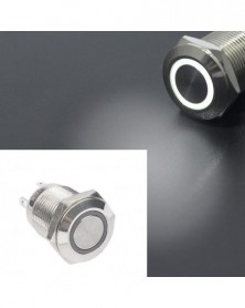
2 key input, provide external input interrupt test function for users to test and debug to use,
External expansion standard 32 bit data bus to provide DMA data transmission capability,
The above functions all provide PCI interface for access and operation, providing DOS, WINDOWS98/WINDOWS
2000 of the WDM driver and the source code for the test program.
With FPGA development board, QUARTUS4.1 and NIOS2 1.01 development tool discs are provided free of charge, and
ALTERA BYTEBLASTER 2 downloads one cable,
The development board supports the AS/PS downloading mode.
Performance and compatibility, stability test
The PCI-E development board is tested on the following PC compatibility machine and runs normally through:
The performance test uses a cyclic maximization transmission method, each DMA block size is 512K bytes, and the average flow rate of 5 seconds is calculated by 1.
How many DMA blocks are transmitted in the second.
CPU memory master chip group operating system DMA read DMA write
P4 2.66G 512M DDR 915P 533 WIN2000/XP FSB 112M bytes / sec 89M bytes / sec
Application scope:
Industrial data acquisition, a/d, d/a data transformation, data processing
Multiple 232/485 extensions, without the need for an external 16c550,1k50 to provide 6 serial ports.
The FIFO of the internal 16C550 can reach 1K bytes
The multiplex switch quantity input / output extension can be extended to 64.
PCI data buffer, data encryption
Industrial control
Specifications
Material
+
Brand Name
XY AMY