- -52%
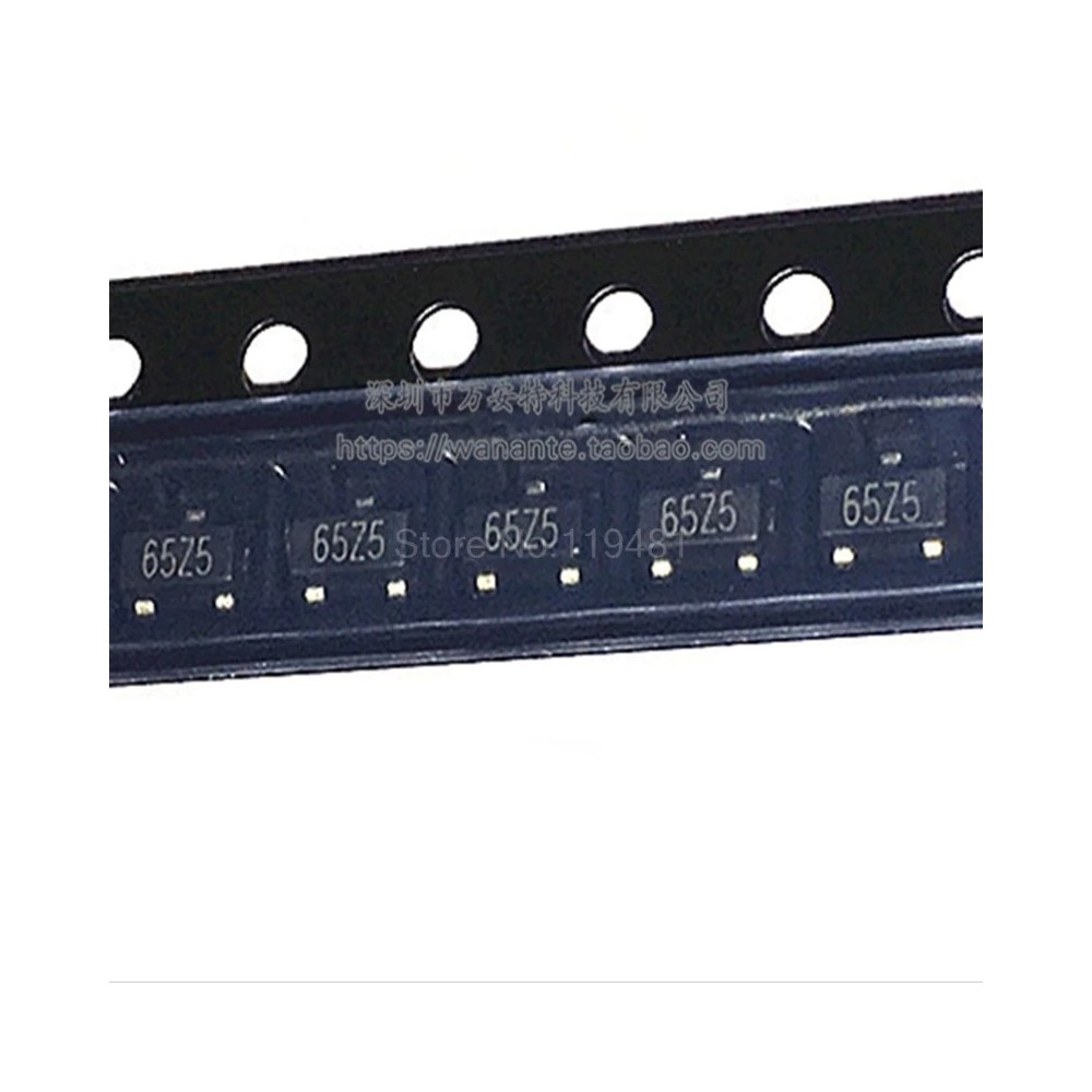
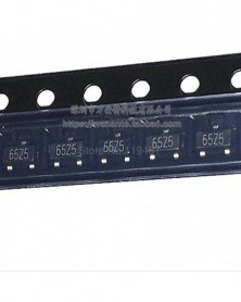

XC6206P302MR vadonatújXC6206P302MR 3.0v 65Z5 szitanyomás sot 23 3v pozitív feszültségszabályozó chip
XC6206P302MR vadonatújXC6206P302MR 3.0v 65Z5 szitanyomás sot 23 3v pozitív feszültségszabályozó chip
57 Ft
52% megtakarítás
119 Ft
Nincs adó
-5
/
 5
A Megtakarítás az Üzletben is Beváltható
5
A Megtakarítás az Üzletben is Beváltható
XC6206P302MR Brand newXC6206P302MR 3.0v 65Z5 silk screen sot 23 3v positive voltage regulator chip
■ GENERAL DESCRIPTION
The XC6206 series are highly precise, low power consumption, high voltage, positive voltage regulators manufactured using
CMOS and laser trimming technologies. The series provides large currents with a significantly small dropout voltage.
The XC6206 consists of a current limiter circuit, a driver transistor, a precision reference voltage and an error correction circuit
The series is compatible with low ESR ceramic capacitors. The currrent limiter's foldback circuit also operates as a short protect for
the output current limiter and the output pin.
Output voltage can be set internally by laser trimming technologies. It is selectable in 0.1V increments within a range of 1.2V to 5.0V.
SOT-23, SOT-89, TO-92 and USP-6B packages are available.
■ APPLICATIONS
● Battery powered equipment
● Reference voltage sources
● Cameras, video cameras
● Portable AV systems
● Mobile phones
● Portable games
● Cordless phones,
wireless communication equipment
■ FEATURES
CMOS
Maximum Output Current Dropout Voltage
Maximum Operating Voltage Output Voltage Range Highly Accurate
Low Power Consumption Operating Temperature Range Low ESR Capacitor
Current Limit Circuit Built-in Ultra Small Package
: 250mA (5.0V type)
: 250mV @ 100mA (3.0V type)
: 6.0V
: 1.2V ~ 5.0V (0.1V increments)
: Fixed voltage accuracy ±2% ( 30mV@VOUT<1.5V)
( 1% @VOUT>2.0V)
: 1.0mA (TYP.)
: -40OC ~ 85 OC
: Ceramic capacitor compatible
: SOT-23 (250mW) SOT-89 (500mW) TO-92 (300mW) USP-6B (100mW)
■ TYPICAL APPLICATION CIRCUIT
■ TYPICAL PERFORMANCE CHARACTERISTICS
PIN ASSIGNMENT
■PRODUCT CLASSIFICATION
● Ordering Information
XC6206P ①②③④⑤
*The dissipation pad for the USP-6B package should be solder-plated in recommended mount pattern and metal masking so as to enhance
mounting strength and heat release. If the pad needs to be connected to other pins, it should be connected to the pin number 4 (VIN).
(TOP VIEW)
DESIGNATOR
DESCRIPTION
SYMBOL
DESCRIPTION
①②
Output Voltage
12~50
: e.g. VOUT: 3.0V→①=3, ②=0
③
Accuracy
2
: Within 2% (within 30mV when VOUT<1.5V)
1 *
: Within 1%
④
Packages
M
: SOT-23
P
: SOT-89
D
: USP-6B
T
: TO-92 (T type)
L
: TO-92 (L type) (Discontinued Product)
⑤
Device Orientation
R
: Embossed tape, standard feed
L
: Embossed tape, reverse feed
H
: Page type (TO-92)
B
: Bag (TO-92)
* 1% accuracy can be set at VOUT(T) > 2.0V.

Szállításii feltételek

Biztonsági feltételek

Visszaküldési feltételek