- -52%
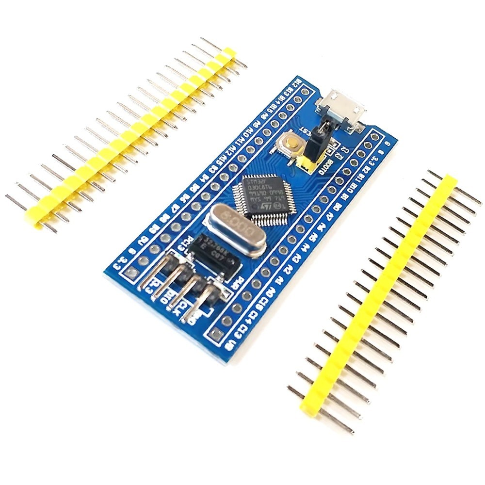
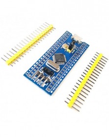
1 db STM32F030C8T6 mikrokontroller fejlesztő kártya kis alaplap tanulótábla kísérleti kártya alaplap
1 db STM32F030C8T6 mikrokontroller fejlesztő kártya kis alaplap tanulótábla kísérleti kártya alaplap
359 Ft
52% megtakarítás
748 Ft
Nincs adó
Product introduction:
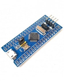
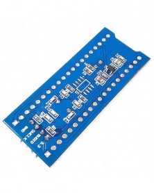
This is an ARM system core board based on STM32F030C8T6 as the main chip, with the power supply circuit, crystal oscillator circuit, reset circuit and program programming circuit. Reasonable circuit design ensures that the MCU can work, which can make it more convenient for users to build on this foundation. Expand your own peripheral circuits. The program can be developed using keil or IAR programming software, and the compiled program can be downloaded through SWD or ISP. The materials and technologies we provide can be used to learn ARM microcontrollers and develop products.
F0 obtains the value of nBOOT1 through the select bit in the user option byte at memory address 0X1FFFF800, instead of using two pins to set it. Together with BOOT0 pin, select boot mode to FLASH storage, SRAM or system memory
①. Main chip (Model: STM32F030C8T6)
1.1. Package type: LQFP;
1.2. Number of pins: 48;
1.3. Kernel: ARM 32-bit CortexⓇ-MO CPU;
1.4. Working frequency: 48MHz;
1.5. Storage resources: 64K Byte Flash/8K Byte RAM;
1.6. Interface resources: 2x SPI, 2x USART, 2x 12C, 39x I/O port
1.7. Analog-to-digital conversion: 1x ADC (12 bits/10 channels)
1.8. Timer: 5x general purpose timer
1x Advanced Timer
1x base timer
1.9. Debug download: Only support SWD debug download.
1.10. Working voltage: 2.4~3.6V
②. Mirco USB interface: power supply and USB communication function, (does not support program download)
③. Start jumping to choose the programming method: (1, user flash memory 2, SRAM 3, system memory).
④. Reset button: used to reset the chip program by the user.
⑤.8M crystal oscillator: The main frequency of the system can be set to 48MHz through frequency multiplication setting.
⑥.32.768KHz crystal oscillator: available for built-in RTC, or for calibration.
⑦. Power LED (PWR): Power indicator status, can judge whether the power supply is stable,
⑧. User LED (PC13): It is convenient for I/O output testing or indicating program running status.
⑨. SWD interface: support simulation, download and debugging.
⑩. RT9193-33: 3. 3V voltage regulator chip, the maximum output is 300mA.
I. Reserved EEPROM interface
Additional instructions:
1. This product has led out the necessary I/O port pins to facilitate connection with peripherals.
2. In addition to downloading through the SWD interface, the program can also be downloaded through USART1 (PA9 and PA10).
3. About the screen printing of the core board:
5V>>Core board system 5V power supply interface, at this time 3.3 (3.3V) is equivalent to output
G>>Power Ground,
VB >> VBAT pin on MCU
A/B/C (0~15)—> the pin number of the GPIO port of A/B/C on the MCU
DIO>>SWDIO (data signal line)
DCLK>>SWCLK (clock signal line)

Szállításii feltételek

Biztonsági feltételek

Visszaküldési feltételek


