- -49%


Szín: DIY Kit - 1Hz-1MHz XR2206 funkciójelgenerátor barkács készlet szinuszos/háromszög/négyzetes kimeneti
Szín: DIY Kit - 1Hz-1MHz XR2206 funkciójelgenerátor barkács készlet szinuszos/háromszög/négyzetes kimeneti
419 Ft
49% megtakarítás
822 Ft
Nincs adó
Features:
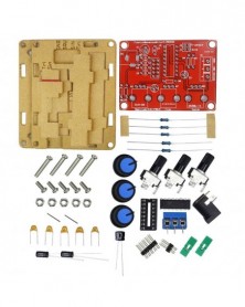
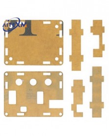
These are all the parts, it need your own welding and installation
Voltage Supply: 9-12V DC Input
Waveforms: Square, Sine & Triangle
Impedance: 600 Ohm 10%
Frequency: 1Hz - 1MHz
SINE WAVE
Amplitude: 0 - 3V at 9V DC input
Distortion: Less than 1% (at 1kHz)
Flatness: 0.05dB 1Hz - 100kHz
SQUARE WAVE
Amplitude: 8V (no load) at 9V DC input
Rise Time: Less than 50ns (at 1kHz)
Fall Time: Less than 30ns (at 1kHz)
Symmetry: Less than 5% (at 1kHz)
TRIANGLE WAVE
Amplitude: 0 - 3V at 9V DC input
Linearity: Less than 1% (up to 100kHz) 10mA
2. The Function Generator component parameter table
Note
label
type
parameters
R1
resistor
1K
Regardless of the polarity
R2
Adjustable resistance
B503=50K
(by screen printing layer)
R3, R5,R6
resistor
5.1K
Regardless of the polarity
R4
resistor
330
Regardless of the polarity
R7
Adjustable resistance
B503=50K
(by screen printing layer)
R8
Adjustable resistance
B104=100K
(by screen printing layer)
C1,
Electrolytic capacitor
100UF
The positive short feet negative long feet
C2
non-polar capacitors
104
Regardless of the polarity
C3,C4
Electrolytic capacitor
10UF
The positive short feet negative long feet
C5
non-polar capacitors
105
Regardless of the polarity
C6
non-polar capacitors
473
Regardless of the polarity
C7
non-polar capacitors
222
Regardless of the polarity
C8
non-polar capacitors
101
Regardless of the polarity
U1
IC
XR2206
(by screen printing layer)
JK1
DC POWER
(by screen printing layer)
J1
2PIN Jumper cap
XM2.54
Regardless of the polarity
J2
2PIN Jumper cap
XM2.54
Regardless of the polarity
P1
Signal wire terminal
(by screen printing layer)
J3
2*5P Jumper cap
3The welding installation considerations, follow these steps:
1. The components are welding the front board, from low to high principles, namely the first low welding components, such as, capacitor, resistor, diode, etc.
2.Welding IC socket, terminal blocks, finally power socket, adjustable potentiometer.
3.The back with a diagonal cutting pliers to cut short the pins as far as possible
4 Debugging steps:
1After completion of welding on IC, XR2206, pay attention to the direction of IC, insert the might damage the chip!
2. check the IC whether against, such as anti please timely correction.
3. Insert the power supply, power supply for 5.5 * 2.1 port, inside outside is negative polarity. For 9-12 v power supply voltage. The waveform may not be stable for more than 12 v
5 Using the step
1. J1 jumper cap plug in, SIN/TRI blue terminals output sine wave (note J1, J2 can only insert one of)
2. J2 jumper cap plug in, SIN/TRI blue terminals output triangular wave (note J1, J2 can only insert one of)
3. SQU blue terminals output pulse
4. AMP : Sine wave, triangle wave amplitude adjustment
5. FINE : Frequency fine adjustment
6. Coarse : Frequency of coarse adjustment
6Schematic diagram of Function Generator

Biztonsági feltételek

Szállításii feltételek

Visszaküldési feltételek