- -52%


PCF8591 AD/DA átalakítása digitális átalakító modul hőmérsékleti megvilágítási moduljának
PCF8591 AD/DA átalakítása digitális átalakító modul hőmérsékleti megvilágítási moduljának
199 Ft
52% megtakarítás
415 Ft
Nincs adó
@past
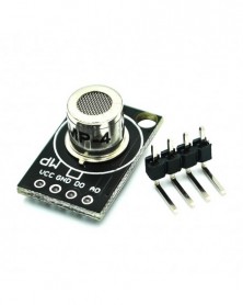
PCF8591 is a single-supply, low-power 8 COMS-type A / D, D / A converter chip, it has a 4-channel analog input channels, all the way to the analog output channels and an I2C bus interface. The device I2C slave address lower three chips A0, A1 and A2, three address pins decision so without adding any hardware with an I2C bus can connect up to eight devices of the same type. The device has a multi-channel analog input, on-chip track-and-hold, 8 A / D conversion and eight D / A conversion functions. A / D and D / A conversion rate determined by a maximum transfer rate of the I2C bus.
Characteristics:
Single power supply;
The normal operating supply voltage range of 2.5V ~ 6V;
Completed through the I2C bus data input / output;
Device address is determined by three address pins;
The sampling frequency is decided by the I2C bus transfer rate;
The 4 Road analog inputs programmable as single-ended or differential inputs;
Can be configured to convert the channel number is automatically increased functionality;
The analog voltage range of VSS ~ VDD;
On-chip track-and-hold function;
8-bit successive approximation A / D conversion;
Multiplication with one analog output D / A converter.
Module Description:
Module chip with PCF8591T, SMD package
Support 4 channel analog voltage the acquisition signal input (voltage input range of 0 - 5V)
Module with power indicator 1 (D1)
A module with DA output indicator (D2), when the DA output voltage reaches a certain value, the indicator light, the higher the voltage value, the brighter lights
The module integrates a Road 0 - 5V voltage input acquisition (through the blue and white potentiometer to adjust the input voltage)
The module Integrated Road the photoresistor (Model: 5537), ambient light intensity by AD collection
Module integrated way thermistor (Model: MF58) ambient temperature by AD collection
PCB size: 48mm * 25mm * 1.6mm
Quality panel corners arc design will not scratch your hand. With a positioning hole aperture 3.1mm, easy to use 3mm Tongzhu fixed
Wiring instructions:
Left 4 pin:
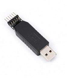
SDA IIC data interface connected microcontroller IO ports (P2.0)
SCL IIC clock interface connected microcontroller IO port (P2.1)
The cathode interface external VCC power 3.3/5V positive power supply
GND Negative interface external 3.3/5V negative supply
Right 8 pin :
AOUT module DA output port
AIN3 analog input signal interface
AIN2 analog input signal interface
AIN1 analog input signal interface
AIN0 analog input signal interface 0
The INPUT3 analog input signal interface 3
INPUT2 thermistor signal input port is connected to
The INPUT1 has photoresistor signal input port connected to the
INPUT0 is connected to the signal input port of the potentiometer
PCF8591 is a single-supply, low-power 8 COMS-type A / D, D / A converter chip, it has a 4-channel analog input channels, all the way to the analog output channels and an I2C bus interface. The device I2C slave address lower three chips A0, A1 and A2, three address pins decision so without adding any hardware with an I2C bus can connect up to eight devices of the same type. The device has a multi-channel analog input, on-chip track-and-hold, 8 A / D conversion and eight D / A conversion functions. A / D and D / A conversion rate determined by a maximum transfer rate of the I2C bus.
Characteristics:
Single power supply;
The normal operating supply voltage range of 2.5V ~ 6V;
Completed through the I2C bus data input / output;
Device address is determined by three address pins;
The sampling frequency is decided by the I2C bus transfer rate;
The 4 Road analog inputs programmable as single-ended or differential inputs;
Can be configured to convert the channel number is automatically increased functionality;
The analog voltage range of VSS ~ VDD;
On-chip track-and-hold function;
8-bit successive approximation A / D conversion;
Multiplication with one analog output D / A converter.
Module Description:
Module chip with PCF8591T, SMD package
Support 4 channel analog voltage the acquisition signal input (voltage input range of 0 - 5V)
Module with power indicator 1 (D1)
A module with DA output indicator (D2), when the DA output voltage reaches a certain value, the indicator light, the higher the voltage value, the brighter lights
The module integrates a Road 0 - 5V voltage input acquisition (through the blue and white potentiometer to adjust the input voltage)
The module Integrated Road the photoresistor (Model: 5537), ambient light intensity by AD collection
Module integrated way thermistor (Model: MF58) ambient temperature by AD collection
PCB size: 48mm * 25mm * 1.6mm
Quality panel corners arc design will not scratch your hand. With a positioning hole aperture 3.1mm, easy to use 3mm Tongzhu fixed
Wiring instructions:
Left 4 pin:
SDA IIC data interface connected microcontroller IO ports (P2.0)
SCL IIC clock interface connected microcontroller IO port (P2.1)
The cathode interface external VCC power 3.3/5V positive power supply
GND Negative interface external 3.3/5V negative supply
Right 8 pin :
AOUT module DA output port
AIN3 analog input signal interface
AIN2 analog input signal interface
AIN1 analog input signal interface
AIN0 analog input signal interface 0
The INPUT3 analog input signal interface 3
INPUT2 thermistor signal input port is connected to
The INPUT1 has photoresistor signal input port connected to the
INPUT0 is connected to the signal input port of the potentiometer

Szállításii feltételek

Biztonsági feltételek

Visszaküldési feltételek